Molecular Nano-Engineering Lab.
TANII Research Group
Fabrication of Nanostructure Array by Ion- Bombardment-Retarded Etching
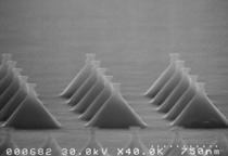
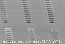
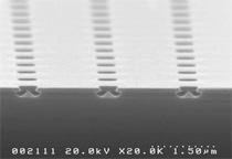
The ion-bombardment-retarded etching phenomenon was discovered first by Dr. Meishoku Koh-Masahara when he studied on the effect of ion-beam-induced damage in silicon in Waseda University as a visiting associate professor. This phenomenon is very unique and is useful for the fabrication of nanostructures. Thus far, nanopyramid arrays, gated silicon field emitter arrays, and double-gate metal-oxide-silicon field-effect-transistors have been fabricated by the ion-bombardment-retarded etching.
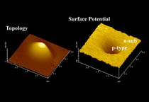
Nano/microstructures are fabricated on a silicon substrate by wet chemical etching using alkaline solutions such as tetramethylammonium hydroxide, hydrazine, and KOH. For the fabrication of a conductive layer of an electronic device, ion implantation is carried out after the etching. The ion-bombardment-retarded etching combines the ion implantation and the silicon etching. Namely, the ion-implanted region can be used as an etching mask for the subsequent wet chemical etching of silicon in alkaline solutions. When ion is implanted into silicon surface, the surface becomes amorphous. The high resistance of this amorphous layer prevents the silicon from electrochemically dissolving in alikaline solution. Thus, the ion-implanted region acts as an etching mask for the wet chemical etching of silicon. Since the etching is independent to the implanted ion species, both n-type and p-type conductive layers can be fabricated on the silicon nano/microstructures as we designed.
M.Koh, T.Goto, T.Iida, A.Sugita, T.Tanii, T.Shinada, T.Matsukawa, I.Ohdomari: Simple Process for Buried Nanopyramid Array (BNPA) Fabrication by Means of Dopant Ion Implantation and Dual Wet Etching, Extended Abstracts of the 2000 International Conference on Solid State Devices and Materials, 2000, 448.
M.Masahara, T.Matsukawa, K.Ishii, Y.Liu, M.Nagao, H.Tanoue, T.Tanii, I.Ohdomari, S.Kanemaru, E.Suzuki: Fabrication of ultrathin Si Channel Wall For Vertical Double-Gate Metal-Oxide-Semiconductor Field-Effect Transistor (DG MOSFET) by Using Ion-Bombardment-Retarded Etching (IBRE), Jpn. J. Appl. Phys. 42, 2003, 1916.
T.Tanii, S.Fujita, Y.Numao, I.Matsuya, M.Sakairi, M.Masahara, I.Ohdomari: A Novel Process for Fabrication of Gated Silicon Field Emitter Array Taking Advantage of Ion Bombardment Retarded Etching, Jpn. J. Appl. Phys. 44, 2005, 5191.